As nanometer-scale circuits move toward single-digit feature sizes, the optical systems used in semiconductor manufacturing to print, inspect, and measure them are being pushed to increasingly narrow tolerance bands. As a result, the optical design parameters across equipment – such as wavelength, surface quality, coating uniformity, and sub-micron assembly precision – can now determine whether an inspection tool detects a defect or misses it entirely.
With 3nm process nodes now in volume production in semiconductor manufacturing, the margin for optical error has effectively disappeared. Equipment that once accepted optical systems with λ/4 wavefront errors now requires λ/10 or better – not as a specification preference, but as a functional threshold at which a system can’t distinguish signal from noise.
Optical Requirements by Semiconductor Manufacturing Application
Semiconductor equipment isn’t a single-wavelength platform; each spectral band presents distinct optical engineering constraints, meaning a component specified for one wavelength range is rarely suitable for another in the same instrument.
Lithography & Alignment
These operations – performed in photolithography equipment – operate in the ultraviolet (UV) spectrum, where fused silica substrates are needed to maintain transmittance, and the coefficient of thermal expansion (CTE) of optical mounts must be controlled to preserve alignment.
Inspection Tools
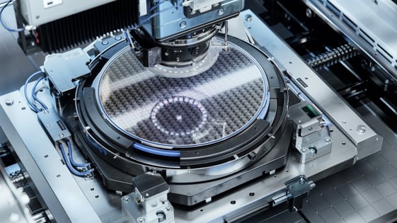
Wafer inspection laser systems typically push into deep-UV (DUV) wavelengths. They’re highly sensitive to surface imperfections that appear negligible at visible wavelengths and generate measurable scatter at DUV, elevating the noise floor and reducing sensitivity to sub-100nm defects.
Metrology
These instruments predominantly use near-infrared (NIR) interferometry, in which the transparency of silicon wafers enables subsurface characterization. Here, the thermal stability of each optic in the beam path is vital, as dimensional drift can disturb the interferometric phase and introduce measurement error.
Optical Component Specifications
Surface flatness, transmitted wavefront error, scratch-dig parameter, and substrate selection govern every optical component in semiconductor manufacturing processes, determining whether a system meets accuracy, throughput, and reliability requirements – or falls short.
- Laser optics: beam steering accuracy and beam delivery precision in wafer inspection and laser processing systems are dependent on the surface flatness of a laser mirror. A mirror held to λ/10 surface flatness preserves beam pointing accuracy – any deviations beyond this limit translate into pointing misalignment at the wafer.
- Lenses: chromatic aberration across the operating spectral range determines whether the focused spot remains within the system’s resolution budget. Achromatic or apochromatic optical designs are typically selected to correct at two or three wavelengths, respectively, depending on the required bandwidth and correction.
- Filters: by controlling in-band transmission and out-of-band rejection, bandpass filters maintain defect contrast and suppress the noise floor
- Plano optics: optical flats, beamsplitter substrates, and windows must be specified to transmitted wavefront error (TWE), rather than surface figure alone
-
Prisms: angle tolerance between faces determines beam deviation accuracy.
Supporting Micro-Scale Tolerances with Thin-Film Coatings & Optical Assemblies
Assemblies
Multi-element optical assemblies – such as doublets, triplets, and other compound configurations – are subject to tilt, decenter, cement uniformity, and CTE – all of which contribute to wavefront distortion and present distinct optical design challenges. Sub-micron accuracy in component alignment is just as critical as individual optic specification.
Tolerances can only be maintained reliably when optical fabrication, coating, and assembly are controlled within a single manufacturing environment, a capability central to our vertically integrated facility. This includes ultra-precision polishing and metrology at all stages of fabrication, supported by in-house optical quality testing using white-light interferometry and non-contact profilometry.
Thin-Film Optical Coatings
The optics in semiconductor manufacturing processes place specific demands on their optical coatings. In multilayer coatings, thickness variations across an aperture can shift spectral response and generate scatter, raising the inspection noise floor and reducing defect detection sensitivity. Coating stress can also introduce surface deformation in thermally cycled environments, distorting beam delivery and shifting the reflected wavefront.
At Torrent Photonics, our optical coating capabilities cover semiconductor handling and laser processing applications, including high-laser-damage-threshold coatings.
Precision Components & Optical Assemblies
Our vertically integrated supply chain reduces inter-supplier risk and maintains tolerance control from specification through production. To explore how Torrent Photonics can support your next project, get in touch with our specialists via the button below.
Microelectronics US 2026
In just a couple of weeks, members of the Torrent team will be in Austin, Texas for Microelectronics US 2026, a completely free event running from April 22nd to 23rd.
Intended for everyone from semiconductor design engineers to packaging and integration specialists, if you work directly on design, fabrication, packaging, integration or manufacturing , then this is the event for you.
If you're planning on attending, be sure to stop the Torrent team to say hi and find out just how our 20+ years of photonics expertise can support you.