
Strip away the robotics and cleanroom environment, and semiconductor manufacturing runs on light. Precision optics project circuit patterns, reveal flaws, and capture measurements that determine whether a wafer passes inspection and moves on to shipment.


The microelectronics industry tends to focus their attention on chips and process nodes, but the equipment that manufactures them determines what’s achievable. At their core, the machines used to pattern, inspect, and measure are precision-engineered instruments containing optical components whose quality defines the limits of the tool's performance. Imperfections that slip past wafer inspection later emerge as failed devices, so detection capability and yield depend on the optics.
To put a number on it: an EUV mirror figured to λ/50 at 13.5 nm carries an absolute wavefront tolerance well under a nanometer, held across a substrate that can exceed 300 mm and still perform after years of thermal cycling and duty. That is the scale advanced fabs are now specifying, and it is why the optics, not only the chips, define what a leading-edge tool can resolve.
The Optical Demands of Lithography, Inspection and Metrology
Every stage of semiconductor manufacturing places different demands on optics. Lithography systems project circuit patterns onto wafers using ultraviolet light. DUV platforms rely on complex refractive lens assemblies, while EUV systems use all-reflective optical architectures because no practical lens material transmits efficiently at 13.5 nm.
As resolution requirements increase, so do the demands placed on optical components. Higher numerical apertures tighten tolerances on surface figure, coating uniformity, alignment, and thermal stability, making optical fabrication and metrology increasingly critical to tool performance.
Inspection tools face a different challenge: detecting ever-smaller defects. Many operate at DUV wavelengths, where optical scatter becomes a significant limitation. Surface figure, roughness, and mid-spatial-frequency errors that have little impact at visible wavelengths can become meaningful sources of noise, reducing sensitivity and contrast.
Metrology systems complete the process by measuring overlay, critical dimensions, film thickness, and process variation. Because these tools establish whether a wafer passes specification, their reference optics must exceed the accuracy of the measurements being made. Any wavefront error, thermal drift, or optical instability directly affects measurement confidence.
Why Surface Accuracy and Consistency Set the Limit
Surface errors on an optic translate directly into wavefront errors in the finished instrument, degrading resolution, overlay accuracy, and beam quality. To remain within system error budgets, semiconductor optics typically require irregularity of λ/10 or better and angstrom-level surface roughness. Coating uniformity is equally important, as thickness variations can shift spectral response and introduce transmitted wavefront error.
For optical engineers, RMS figure alone rarely tells the whole story. Performance is often governed by the spatial-frequency content of the surface. Low-frequency figure errors affect imaging performance, while mid-spatial-frequency errors left by fabrication processes scatter light close to the main beam and can become a limiting factor in lithography, inspection, and metrology systems. High-frequency roughness contributes to wide-angle scatter and reduced image contrast. An optic may meet its figure specification yet still underperform if mid-spatial-frequency content is not tightly controlled.
Equally important is repeatability. Semiconductor equipment manufacturers require optical performance to remain consistent across production volumes, not just prototypes. The challenge is therefore not only achieving specification once but reproducing it reliably from the first optic to the hundredth.
Material selection supports that stability. Fused silica, Ultra-Low Expansion (ULE®) glass, and Zerodur are commonly specified because their low thermal expansion helps maintain figure under changing operating conditions. In polarisation-sensitive metrology systems, residual stress birefringence can also introduce measurement error, making stress-relief processing and birefringence testing critical parts of the fabrication process.
Where Aspheric Lenses Offer an Advantage
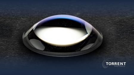
Spherical aberration occurs when a spherical surface refracts marginal rays more strongly than paraxial rays, causing them to focus at different points. Because an asphere's profile is a controlled departure from a sphere, it can correct this effect and often replace multiple spherical elements. Fewer optical interfaces can reduce stray light, simplify alignment, shorten optical trains, and enable more compact designs.
Our high-precision aspheric lenses are fabricated to better than λ/20 irregularity and surface roughness below 0.3 nm RMS. These capabilities support demanding applications including semiconductor inspection, alignment optics, metrology systems, and precision beam delivery.
Achieving λ/20 irregularity on a surface with continuously varying curvature requires specialised fabrication processes. At Torrent Photonics, asphere fabrication begins with CNC grinding to generate the base profile, followed by sub-aperture polishing to refine the surface toward its final figure. Where residual errors remain, Magnetorheological Finishing (MRF) is used to improve surface accuracy and reduce artefacts. Verification is performed using interferometry and non-contact profilometry to confirm that the finished optic conforms to specification.
Supporting the Semiconductor Supply Chain
For OEMs, the optical supply chain shapes what a finished tool can deliver. Our precision optics fabrication, thin-film coatings for semiconductor handling and processing, and wafer-level coating services support equipment builders from prototype through volume manufacturing, backed by ISO 9001, AS9100D, and ITAR-registered quality procedures.
That fabrication discipline extends to how optics are handled and integrated downstream. Surface cleanliness is typically called out to scratch-dig standards such as MIL-PRF-13830, particle counts are controlled through coating and assembly, and mechanical references (centration, wedge, and mounting-surface runout) are held tightly enough that an optic drops into its opto-mechanical mount without re-aligning the whole beam path on the bench.
To discuss the optical requirements for your application, please contact our technical team.