
Optical filters don't have to be a separate part in front of the sensor. Patterned directly on a wafer, a filter can sit right at the image plane, which can reduce package size and system complexity.
This article explains how that works. It covers how patterned filters are made on a wafer with photolithography, an approach often called wafer-level processing (WLP), where it is already used in volume, and what it offers designers of machine vision and automated optical inspection (AOI) systems.
Why put the filter on the wafer
A filter bonded to the sensor, or patterned onto it, sits right at the image plane. There is no gap between filter and pixel, one fewer optical interface to align, and a smaller package overall. Because the pattern is made with the same batch processes used for semiconductor devices, it can also be repeated across a whole wafer and from one wafer to the next.
For compact systems, that is a real advantage. Our earlier post on why optical filtering matters in compact imaging systems covers the design case. Here we look at how the filters are made.
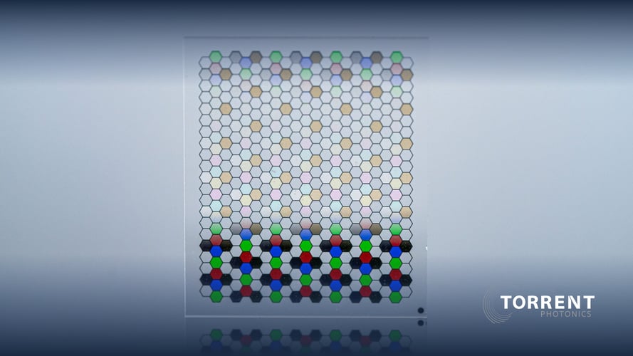
How A Patterned Filter is Made On A Wafer
The exact process depends on the filter type and the application. These are the main capabilities involved in patterning a filter on a wafer:
- Prepare the wafer. We process customer-supplied wafers up to 8 inches, and we can pattern on glass as well as semiconductor wafers. For color resists, we use wafer planarization so the pattern resolves on surfaces with drastic topography.
- Apply the filter material. There are two main routes. Color resists give RGB or CYM spectral performance and come with UV-cure and low-heat options. Dichroic coatings give NIR, visible, and UV filter performance and are deposited by ion-assisted deposition (IAD) evaporation, magnetron sputtering, or ion beam sputtering.
- Pattern with lithography. Semiconductor-style mask aligners in our lithography fab handle wafers up to 8 inches and support ultra-small, micrometer-scale pixel-level features for imaging applications. Alignment accuracy and alignment markers are among the design parameters we define with each customer.
- Keep the sensor clean. The process is designed to keep dark-current contamination to a minimum, and it runs in Class 100/1000 wafer fabrication cleanrooms built for micropatterned coatings. Dicing, testing, and packaging are handled to the customer's specification.
Where It Is Used Today
Our active wafer deposition service supports high-volume production for the semiconductor and cell phone industries, including processing of customer-supplied wafers. The main benefit is better signal-to-noise on ambient light, proximity, and biometric sensors.
The reason is straightforward. A proximity or biometric sensor needs to see the wavelength of its own emitter and as little else as possible. An ambient light sensor needs a spectral response that tracks what the eye sees. Patterning the filter on the wafer lets each sensor get the response it needs without an extra optical part in the stack.
What It Means for AOI and Machine Vision
Many inspection setups gain contrast by imaging a part under more than one color or wavelength. Doing that one band at a time, with a filter wheel, several cameras, or repeated exposures, costs throughput and adds alignment work. On a moving line, the extra time and motion can also hurt accuracy.
A patterned filter on the sensor offers another route:
- One exposure, several bands. Bayer, stripe, and mosaic layouts, often grouped under the name multispectral filter arrays (MSFAs), capture multiple spectral bands at once. We can pattern up to 9 bands on one substrate, on glass or on semiconductor wafers.
- Fewer parts. Multiple bandpass filters on one substrate for one camera can remove the need for several cameras in one system.
- Bands that line up. All bands come from the same sensor in the same frame, so they are co-registered by design.
- A smaller footprint. That helps in tight tool spaces and compact inspection heads.
There is a trade-off to plan for. Each band samples only a share of the pixels, so spatial resolution and light per band go down as the band count goes up. The best layout depends on the defect you need to find, which is why we work backwards from the inspection task to the band count.
If you already have a camera you want to adapt, our image sensor modification service can prepare the sensor surface for filters and other optics.

What To Specify
We start each project with a short list of decisions. Having these in hand speeds up a feasibility assessment:
|
Decision |
What to define |
|
Substrate |
Semiconductor wafer, optical-grade glass, fused silica, or another material |
|
Number of bands |
How many filter bands share one substrate |
|
Filter design |
Transmission bands and blocking specifications |
|
Feature geometries |
Smallest feature size and position tolerance |
|
Alignment |
Alignment accuracy and available alignment markers |
|
Handling, testing, packaging |
ESD handling, dicing, finishing, testing and packaging |
Talk to our Lithography Team
Whether you need filters for a wafer-level sensor, a multiband inspection camera or something in between, our engineers can assess technical feasibility and propose a route.
Visit our website to find out more about our discrete patterning and micropatterned filter capabilities.
To start a project, request a quote or contact our technical sales team: sales@torrentphotonics.com.